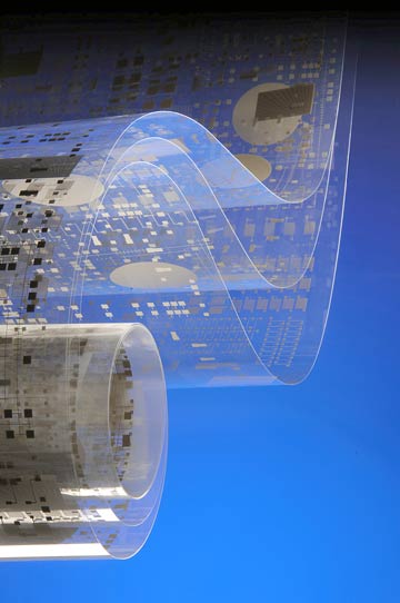
공지 | X-LIGHT 광소결 / 광신터링 / 광솔더링 시스템 (X-LIGHT SINTERING SYSTEM)
페이지 정보
작성자 디티엑스 작성일18-09-17 19:10 조회972회 댓글0건본문
X-LIGHT 광소결 / 광신터링 / 광솔더링 시스템 (X-LIGHT SINTERING SYSTEM)
PHOTONIC CURING, SINTERING, SOLDERING TECHNOLOGY
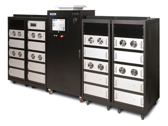
|
|
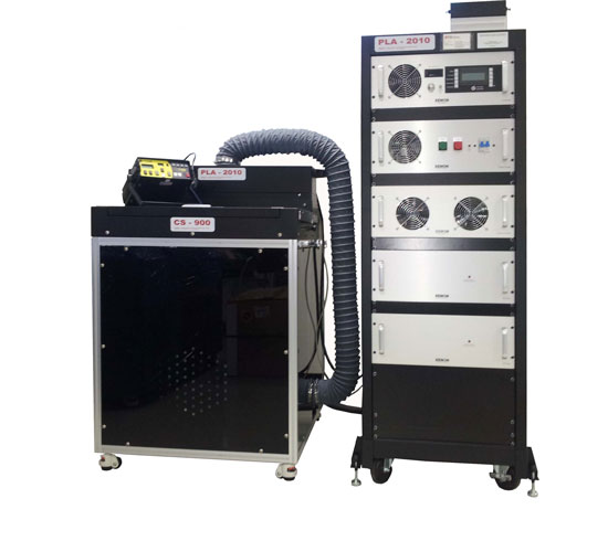
Model : S-5100
|
|
Model : S-2300
|
|
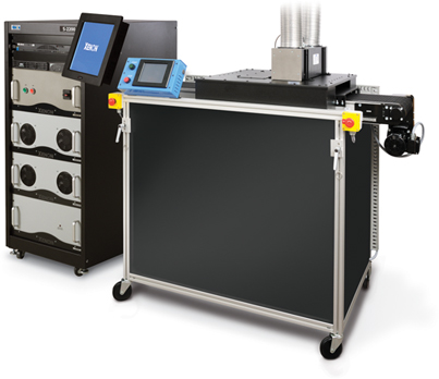
Model : S-2100
|
|
|
|
|
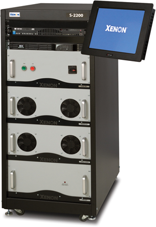
Model : S-2200
|
|
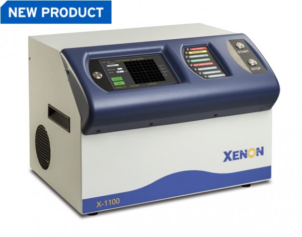
Model : X-1100 (실험용)
|
|
|
|
|
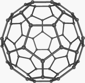
- All materials have basic properties
- Melting point, light absorption (color) etc.
- Governed by laws of particle physics
- These are independent of particle size
- Melting point for a gram of copper is the same as for a kg of Copper. It still looks like the same material
|
|
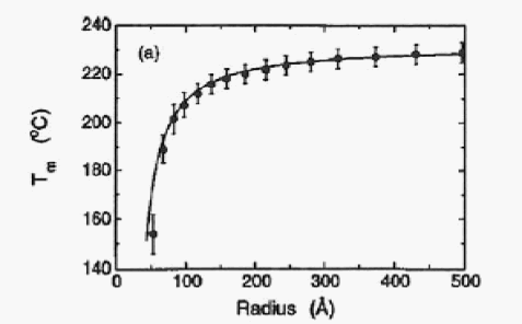
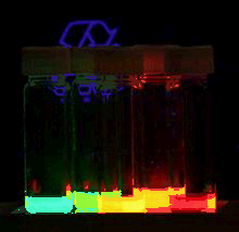
- Basic Principle
- Start with nanoparticle conductive ink
- Deposit on substrate
- Use low temperature to achieve sinter
- Convert to Bulk conductive material,
- nanoparticle properties change
- Melting point, color etc.
- Two different categories of conductive nano inks
- Basic Sintering –e.g. Silver
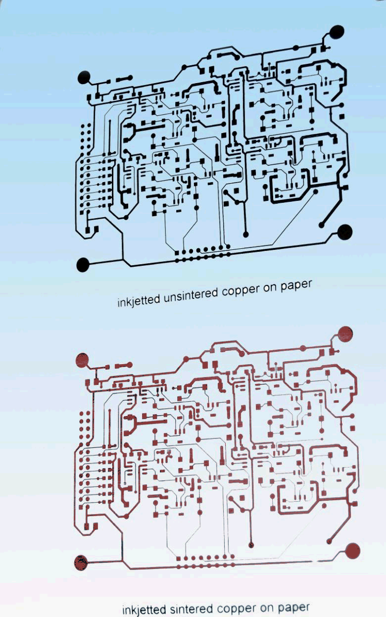
- Reduction and Sintering –e.g. Copper
- Why Sinter Conductive Inks
- Melting point of metals are usually higher than plastics (the substrate)
- Would make conductive traces (printed circuits) onflexible materials
- Could be applied by regular printing process like roll to roll or inkjet.
|
|
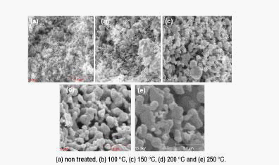
- Silver is relatively easy to sinter
- Silver is Conductive as is Silver Oxide
- Nanomaterial is easy(er) to produce
- Yield is high even if bulk is expensive
- Energy required is low nanoparticle size 5-
- Traditional process.
- Use 120 C thermal for around 10 minutes.
- Shiny finish good conductivity.
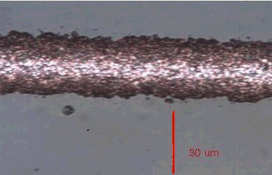
- Using X-Light Lamp
- Excellent Conductivity
- Matt finish due to rapid formation
|
|
- Copper is conductive, Copper oxide not a good conductor. Copper readily oxidizes
- Nanomaterials are harder to produce
- Yield is low even if bulk is cheaper
- Energy required is significantly higher
- Is the “Holy Grail” for Printed electronics technology
- Typically Sintering also requires a reduction of copper oxide to copper.
- Some Oxidizing material in the ink may be required
- Small margin between energy to sinter and energy to evaporate material
|
|
|
|
|
|
|
- In addition to low temperature curing, there are additional benefits of X-Light curing that make it suitable for printable electronics.
- By reducing the time to cure milliseconds, X-Light curing can be compatible with high-speed printing processes such as gravure and flexography without a large amount of dedicated floor space. In essence, the time to cure becomes matched to the time to print.
- The process is suited to nanoparticle-based materials, which also makes it well-suited to high resolution deposition methods and applications.
- The speed with which sintering occurs makes it possible to cure copper in air, which normally must be cured in an inert or reducing environment.
- Once a material has been sintered, it will typically no longer absorb light. Thus there is the potential for building multilayer circuitry that does not thermally stress the underlying layers.
관련기술이 필요하신분은 당사로 문의주시기 바랍니다 !!
TEL : 031-497-1134


 시스템
외관 (APPEARENCE)
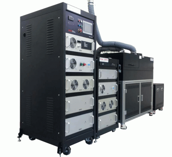
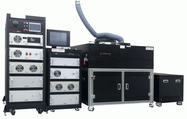
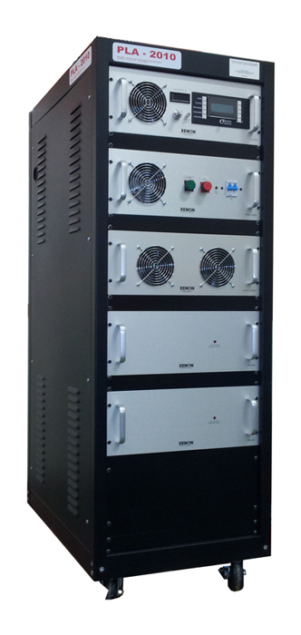
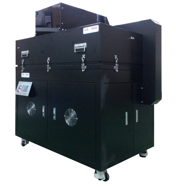
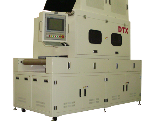
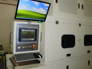
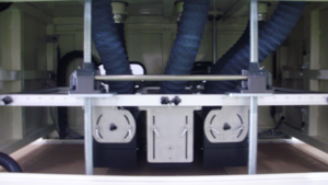


 SINTERING
SILVER NANO PARTICLES
 COPPER
SINTERING
